Bogdan MIEDZINSKI, Grzegorz WISNIEWSKI, Nickolay I. GRECHANYUK, Andrzej GRODZINSKI, Artur KOZLOWSKI
Wroclaw University of Technology (1), Scientific and Producing Company "Eltechmach", Vinnitsa, Ukraine (2),
Tele & Radio Research Institute, Warszawa (3), Institute of Innovative Technologies, EMAG, Katowice (4)
Abstract. Paper presents and discusses investigated results of performance of selected low voltage vacuum interrupters in which the multicomponent multilayer condensed contact material based on Cu-W compositions was used. On the basis of the switching test results followed by respective inspections of the contacts surface and investigations of the microanalysis as well as material morphology the conclusions on possibility of application of such the matehal composition for L V vacuum interrupters in practice are formulated.
Streszczenie. Przedstawiono i omdwiono wyniki badah komdr prdzniowych przeznaczonych do stycznika niskiego napiqcia, w ktdrych zastosowano nakladki stykowe Cu-W wykonane me todq kondensacji warstw wielosktadnikowych. Na podstawie testdw Iqczeniowych oraz analizy powierzchni i skladu chemicznego sformufowano wnioski dotyczqce mozliwoSci zastosowania takich matehafow w niskonapiqciowych komorach gaszeniowych.
Keywords: vacuum interrupter, multilayer condensed multicomponent material, electrical contact
Slowa kluczowe: komora gaszeniowa, wieloskfadnikowy materia} uzyskany metoda kondensacji, kontakt elektryczny
Introduction
Fine powder sinters based on copper - tungsten - chromium composition are commonly used as contact materials in guenching chambers of a low voltage vacuum switchgear. However, fine powder metallurgy is a sophisticated as well as money and time consuming technology. Therefore, to replace it by another effective process engineering is both technically and economically justified. The electron beam high-rate evaporation method with following condensation in vacuum seems to be one of such technologies. It has been successfully applied for fabrication of various multilayer composite materials of different thickness up to about 5 mm in Scientific and Production Enterprise ELTECHMACH in Vinnitsa, Ukraine, and used for various arcing contacts [1-4]. This paper presents and discusses switching properties of low voltage vacuum interrupters (1000V, 400A, 50Hz) in which selected multilayer condensed multicomponent material based on Cu-W composition (W from 5% to 60% in mass) with some impurities like Fe was used. When rated and short circuit tests were completed, the contacts surface inspection followed by respective investigations of the material morphology and its microanalysis were performed using electron microscopy together with appropriate spectroscopy (SEM, XRF, EPMA etc.).
Modern electron beam technology for fabrication of metal compositions
Development of the electron beam technology runs among others along three main ways:
- melting and evaporation in vacuum to produce pure metal ingots, compound alloys, coverings and composition materials,
- welding of metals,
- precise treatment of materials (like drilling, milling and cutting).
SPC "ELTECHMACH" has focused its attention on development of the electron beam equipment to implement this technology for different applications like: deposition on gas turbine blades to perform the thermal barrier, fabrication of composite materials of dispersion-strengthen, microlayers and microporous types, as well as processing of pure metals, preparation of special alloys, ferroalloys and polycrystalline silicon. Therefore, development of laboratory and electron beam equipment was of main importance. One of the most significant achievement is development of the advanced technology for formation of microlayers (sandwich type) materials of thickness of the alternating layers less than 0.5 pm at temperature higher by about 30% of the melting point of the most fusible materials being evaporated [5]. Up to now similar materials were produced by the electron beam evaporation and subsequent condensation of metals and non-metals in vacuum at substrate temperature not higher than 300°C [6], Therefore, it was possible to introduce the innovative electron beam technology to produce relatively thick (up to about 5 mm) microlayers composite materials (Cu-Zr-Y)/Mo for arcing contacts [1,3]. They successfully passed the ratification procedure and are named "the materials dispersion- strengthen for electrical contacts (DSMC)". Since they do not contain silver, their price is lower by about 2.5 - 3 times comparing to the silver based powder electro contacts. On the contrary their switching capacity and life are much higher by about 50%-200%.
At the same time within the framework cooperation of Institute of Problems for Material Science NASU in Kiev, Ukraine and Wroclaw University of Technology, the new materials based on copper, chromium, tungsten and/or molybdenum composition were developed and successfully involved in sliding contacts for the copper mine transportation [3]. Therefore, in the next step an attempt at application of the composite materials for electrical contacts in low voltage vacuum switchgear was made.
Selection of contact samples
New multicomponent composite material was intended for use in vacuum chambers of MVK 400 type (produced in Institute of Tele- and Radiotechnics in Warsaw, Poland) for low voltage interrupters (1000V, 400A, 50Hz) applicable mostly in coal mines. The main goal was to reduce the cost of manufacturing since the contacts made of fine powder sinters (Cu-W) contribute about 30% to the total product price as it can be seen in Fig. 1. (it should be noted also that the multilayer contacts made of Cu-W are found to be cheaper by about (1.3-2) times with compare to the powder-metals).
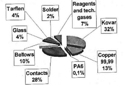
Fig. 1 Share in the cost for vacuum chamber MVK400.
In the first stage, the contact samples of about 0.6mm of thickness were prepared for further processing. Unfortunately, they were found to be mismatched due to thermal stress. Fig. 2 shows that after soldering to the contact base under following processing at elevated temperature (at 800°C), the soldered joints were destroyed indicating partial separation of the boundary layer.
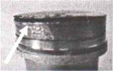
Fig. 2 Partial separation of the contact sample (0,6 mm)
under manufacturing (at 800°C).
Therefore, for further investigation the thickness of the contact samples was increased up to 5mm. They passed the manufacturing process successfully and were assembled as the contacts sets into vacuum chambers of the low voltage interrupters for further switching tests. Since, the contact material for vacuum interrupters must be selected carefully to fulfil contradictory requirements according, among others, to contact resistance, value deterioration of vacuum under operation, mechanical and electrical strength as well as current chopping level [7] therefore, two lots of the contact samples were prepared for testing. First one was made of a high purity copper and tungsten material without any other additives (Table 1) to check first of all the contact resistance value and the vacuum deterioration (leakage current) under rated operation. While, for the second lot iron was especially involved as an alloy addition and both the copper and tungsten ingots were of technical purity. Therefore, one can see another metallic and nonmetallic impurities as indicated in Table 2.
In a case of the pure (Cu-W) composition the maximum amount of tungsten was found to be below 22% to obtain mechanically stable contact structure. Otherwise, it was easy destroyed due to delaminating under mechanical stress (as in Fig.2). To overcome this problem and to increase amount of tungsten to about (30-60)% of mass both water-cooled and non-cooled interlayers of a selected alloy addition must be deposited.
The investigations of mechanical properties of the multilayer compositions based on Cu-W have revealed their advantage over powder materials. The mechanical strength was found to be higher by about 1.5-2 times.
Switching capacity test
The switching test was performed under both rated and short circuit conditions of operation. Circuit diagram and view of the test stand is shown in Fig. 3. Electrical parameters of the test are listed in Table 3.
Under the test not only the voltage across the contact gap and the load current value were measured. The frequency, power factor, source voltage for all phases of the 3-phase system, driving current and displacement of the contact moving system were controlled for better evaluation of the switch performance. It was found that all vacuum chambers successfully passed the rated switching test. They were able to make ("C") and to break ("O") the rated current of 400 A rms successfully for one hour continuous operation independently on the contact sample applied. Performance of the selected chamber under switching ("CO") rated load (single A phase) can be compared in Fig. 4. The vacuum chambers with the contacts made of Cu-W composition but with higher amount of tungsten (up to about 55%) and with iron as an agent (around 0.6%) were also able to successfully pass the short circuit test at 4.5 kA however only for breaking ("O") what is presented in Fig. 5. (load current was delivered to the contacts under the test by means of an auxiliary switch, see Fig. 3). Note, that switching overvoltage level both under rated as well as short circuit conditions was negligible.
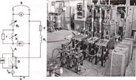
Fig. 3 Circuit diagram and view of the switching test stand.
S-supply,Ur1,Ur2-voltage meters, A-auxiliary switch, Ri, X-resistive and inductive controllers, F-high power fuse, RL-ground current limiter, D-contactor under test, h-current meter, r-shunt, B-link for graduation
Table 1. Material composition (percentage by weight) for the
first lot of the contacts.
|
No of contact |
Cu |
W |
||||
|
Mean |
Max. |
Min. |
Mean |
Max. |
Min. |
|
|
8 |
78.17 |
85.02 |
73.36 |
21.83 |
26.64 |
14.98 |
|
10 |
89.57 |
93.66 |
85.07 |
10.43 |
14.93 |
6.34 |
|
13 |
94.78 |
97.38 |
92.99 |
5.22 |
7.01 |
2.63 |
Table 2. Material composition (percentage by weight) for the
second lot of the contacts.
|
|
Cu |
W |
Fe |
Cr |
Co |
Si |
Al |
|
11 |
75.3 |
23.4 |
0.59 |
0.034 |
0.016 |
0.33 |
0.13 |
|
14 |
61.9 |
36.7 |
0.62 |
0.042 |
0.024 |
0.3 |
0.15 |
|
18 |
44.4 |
54.2 |
0.6 |
0.049 |
- |
0.47 |
- |
Table 3. electrical parameters of the switching capacity
test.
|
Type of test |
Voltage |
Current |
Frequency |
Power factor |
Number of cycles per hour |
|
[V] |
[kA] |
[Hz] |
[-] |
[-] |
|
|
Rated "CO" (close- open) |
1000 |
0.4 |
50 |
0.35 |
120 |
|
Short-circuit "O" (open) |
1000 |
4.5 |
50 |
0.35 |
- |
|
Short- circuit "CO" (close- open) |
1000 |
4.5 |
50 |
0.35 |
- |
On the contrary, with the decreased amount of tungsten (below 22% Table 1) the switch failed in operation already at second breaking cycle. All of them independently on the material composition were damaged immediately under making and following breaking ("CO") of 4.5 kV rms due to contact welding. Tendency for the contact sticking with the increased load current value can be seen when compare the releasing time in transient of the switch driving system (x) with this under effective current breaking presented in Fig. 4 and Fig. 5 respectively.
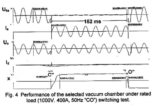
Uka-voltage across the contact, l3-load current, Ua-voltage of the source in A-phase, Ia-confactor driving current, X-disptacement of the contact moving system.
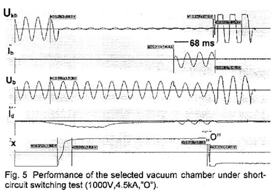
Ukb-voltage across the contact, ib-load current, Ub-voltage of the source in B -phase, Ij-contactor driving current, X-dispiacement of the contact moving system
Contact surface inspection and failure analysis
Inspections (before the switching test) of the contact surface and of the cross section for the selected samples have indicated much more uniform distribution of elements (Cu, W) for the first lot in comparison with the second one, as it can be seen in Fig. 6 and Fig. 7. More detailed investigations revealed non uniform distribution of particular metallic elements (for the second lot of the contact samples) as on the surface and inside the contact volume. The tungsten particles were also found to be largest just at the surface and close to the middle of the contact volume. Both various microstructure and variety of chemical compositions indicated some instabilities of the technology under processing. In spite of that, the vacuum interrupter equipped with the contact samples of the second lot due to the higher amount of tungsten (up to 54%) and iron (-0.6%) as controlling additive was able to operate successfully at breaking of the short circuit current.
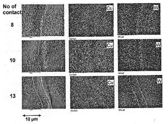
Fig. 6 Elements distribution for selected areas of the contact volume cross-section (first lot see Table 1).
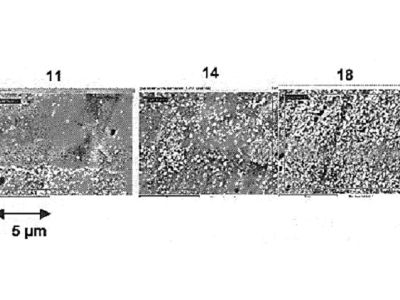
Fig. 7 Wolfram distribution at selected areas of the contact volume cross-section (second lot - see Table 2).
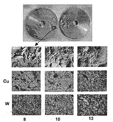
Fig. 8 Appearance of the contact surfaces (for the first lot) after welding under breaking of the short circuit current equal to 4.5kA (1000V, 50Hz, pf 0.35), morphology of the contact surface inside the welded area and surface microanalysis (by means of EDX) over the welded areas.
However it failed in operation under the short circuit ("CO") type of test (see Table 3) but not at the first attempt. On the contrary for the contacts indicating of much more uniform distribution of the metallic elements (Cu, W) but with the decreased amount of tungsten and without respective interlayer alloy additions the hazard of weldability increased respectively. Morphology of the welding area and distribution of both copper and tungsten over this area is presented for example in Fig. 8. Therefore, the contact material based on Cu-W composition and fabricated by means of the electron beam high-rate evaporation method with following condensation in vacuum seems to be promising for electrical contact operating in low-voltage vacuum switchgear. However to meet requirements if about short-circuit capacity, this technology must be improved to increase both amount of tungsten and respective alloy additions to control the current chapping level.
Conclusions
First attempt of use of the multicomponent material made by means of the electron beam high-rate evaporation method with following condensation in vacuum as the contact material for the low voltage vacuum switchgear has indicated its promising properties. The vacuum interrupters were able to operate successfully under rated load (1000V, 400 A, 50 Hz, pf 0.35) however, failed in operation under
short current conditions (1000 V, 4.5 kA, 50 Hz, pf 0.35). ' From the investigated results of both electrical and mechanical properties as well as of surface and volume failure analysis one can conclude that with the increase of amount of tungsten and application of respective interlayer additions this multilayer condensed material can be competitive to the contact materials based on the fine powder technology from both technological and economical perspective.
References
[1] Grechanyuk N.I., Osokin V.A., Grechanyuk I.N., Minakova R.V.: Composite materials on base of copper and molybdenum, condensed from vapor phase for electrical contacts. Structure, properties, technology. Advances in Electrometallurgy No2, 2005, pp. 24-29.
[2] Grechanyuk N.I., Kucharenko P.P., Grechanyuk I.N.: New electron beam equipment and technologies of producing advanced materials and coating. Paton Welding Journal No5, 2007, pp. 25-29.
[3] Miedzinski B., Okraszewski Z., Grechanyuk N.I., Wandzio J.: Performance of sliding contacts with Cu-Mo layers for transportation in mining industry. Electrical Contacts and Electrodes, Izd. IPM NANU, Kiev, 2008, pp. 150-155.
[4] Grechanyuk N.I., Miedzinski B., Grodzinski A.: Modern electron beam technologies for fabrication of various materials powder and metal compositions from a vapour phase. Electrical Review, R.86, No5/2010 pp. 1-4.
[5] Grechanyuk N.I.: Method of production of microlayer thermostable materials. Patent 2271404 RF (Publ. 03.10.2006).
[6] lllinsky A.I.: Structure and strength of lamellar and dispersion strengthened films, Metalurgiye 1986 pp. 140 (in Russian)
Slade P.G.: The vacuum interrupter theory, design and application, CRC Press 1 edition, 2007